Atmel ATmega128RFA1еҚ•зүҮIEEE 802.15.4и§ЈеҶіж–№жЎҲ
Atmel е…¬еҸёзҡ„ATmega128RFA1жҳҜдҪҺеҠҹиҖ—еҚ•зүҮIEEE 802.15.4и§ЈеҶіж–№жЎҲ,йӣҶжҲҗдәҶеҹәдәҺAVRеўһејәзү№жҖ§RISCжһ¶жһ„зҡ„CMOS 8дҪҚMCUд»ҘеҸҠ2.4GHz ISMйў‘ж®өзҡ„й«ҳж•°жҚ®йҖҹзҺҮ收еҸ‘еҷЁ.еҷЁд»¶зҡ„еҗһеҗҗйҮҸиҫҫеҲ°1MIPS/MHz,ж— зәҝз”ө收еҸ‘еҷЁзҡ„ж•°жҚ®ж•°жҚ®йҖҹзҺҮд»Һ250kbpsеҲ°й«ҳиҫҫ2Mbps.ATmega128RFA1е№ҝжіӣеә”з”ЁеңЁZigBee®/IEEE 802.15.4-2006/2003™, RF4CE, SP100, WirelessHART™,ISMеә”з”Ёд»ҘеҸҠIPv6/6LoWPAN.жң¬ж–Үд»Ӣз»ҚдәҶATmega128RFA1дё»иҰҒзү№жҖ§,ж–№жЎҶеӣҫ, AVRжһ¶жһ„ж–№жЎҶеӣҫ, 收еҸ‘еҷЁж–№жЎҶеӣҫд»ҘеҸҠеҹәжң¬еә”з”Ёз”өи·Ҝеӣҫе’Ңжқҗж–ҷжё…еҚ•(BOM)дёҺжү©еұ•зү№жҖ§зҡ„еә”з”Ёз”өи·Ҝеӣҫ.
The ATmega128RFA1 is a low-power CMOS 8 bit microcontroller based on the AVR
enhanced RISC architecture combined with a high data rate transceiver for the 2.4 GHz
ISM band. It is derived from the ATmega1281 microcontroller and the AT86RF231 radio
transceiver.
By executing powerful instructions in a single clock cycle, the device achieves throughputs approaching 1 MIPS per MHz allowing the system designer to optimize power consumption versus processing speed.
The radio transceiver provides high data rates from 250 kb/s up to 2 Mb/s, frame handling, outstanding receiver sensitivity and high transmit output power enabling a very robust wireless communication.
The AVR core combines a rich instruction set with 32 general purpose working registers. All 32 registers are directly connected to the Arithmetic Logic Unit (ALU). Two independent registers can be accessed with one single instruction executed in one clock cycle. The resulting architecture is very code efficient while achieving throughputs up to ten times faster than conventional CISC microcontrollers. The system includes internal voltage regulation and an advanced power management. Distinguished by the small leakage current it allows an extended operation time from battery.
The radio transceiver is a fully integrated ZigBee solution using a minimum number of external components. It combines excellent RF performance with low cost, small size and low current consumption. The radio transceiver includes a crystal stabilized fractional-N synthesizer, transmitter and receiver, and full Direct Sequence Spread Spectrum Signal (DSSS) processing with spreading and despreading. The device is fully compatible with IEEE802.15.4-2006/2003 and ZigBee standards.
ATmega128RFA1дё»иҰҒзү№жҖ§:
• High Performance, Low Power AVR® 8-Bit Microcontroller
• Advanced RISC Architecture
- 135 Powerful InstructionsвҖ“Most Single Clock Cycle Execution
- 32x8 General Purpose Working Registers
- Fully Static Operation
- Up to 16 MIPS Throughput at 16 MHz and 1.8V
- On-Chip 2-cycle Multiplier
• Non-volatile Program and Data Memories
- 128K Bytes of In-System Self-Programmable Flash
• Endurance: 2000 Write/Erase Cycles @ 85в„ғ
- 4K Bytes EEPROM
• Endurance: 2000 Write/Erase Cycles @ 85в„ғ
- 16K Bytes Internal SRAM
• JTAG (IEEE std. 1149.1 compliant) Interface
- Boundary-scan Capabilities According to the JTAG Standard
- Extensive On-chip Debug Support
- Programming of Flash EEPROM, Fuses and Lock Bits through the JTAG interface
• Peripheral Features
- Multiple Timer/Counter & PWM channels
- Real Time Counter with Separate Oscillator
- 10-bit, 330 ks/s A/D Converter; Analog Comparator; On-chip Temperature Sensor
- Master/Slave SPI Serial Interface
- Two Programmable Serial USART
- Byte Oriented 2-wire Serial Interface
• Advanced Interrupt Handler
• Watchdog Timer with Separate On-Chip Oscillator
• Power-on Reset and Low Current Brown-Out Detector
• Advanced Power Save Modes
• Fully integrated Low Power Transceiver for 2.4 GHz ISM Band
- Supported Data Rates: 250 kb/s and 500 kb/s,1 Mb/s, 2 Mb/s
- -100 dBm RX Sensitivity; TX Output Power up to 3.5 dBm
- Hardware Assisted MAC (Auto-Acknowledge, Auto-Retry)
- 32 Bit IEEE 802.15.4 Symbol Counter
- Baseband Signal Processing
- SFR-Detection, Spreading; De-Spreading; Framing ; CRC-16 Computation
- Antenna Diversity and TX/RX control
- TX/RX 128 Byte Frame Buffer
• Hardware Security (AES, True Random Generator)
• Integrated Crystal Oscillators (32.768 kHz & 16 MHz)
• I/O and Package
- 38 Programmable I/O Lines
- 64-pad QFN (RoHS/Fully Green)
• Temperature Range: -40в„ғ to 85в„ғ Industrial
• Supply voltage range 1.8V to 3.6V with integrated voltage regulators
• Ultra Low Power consumption (1.8 to 3.6V) for Rx/Tx & AVR: <18.6 mA
- CPU Active Mode (16MHz): 4.1 mA
- 2.4GHz Transceiver: RX_ON 12.5 mA/TX 14.5 mA (maximum TX output power)
- Deep Sleep Mode:<250nA @ 25в„ғ
• Speed Grade: 0вҖ“16 MHz @ 1.8вҖ“3.6V
ATmega128RFA1еә”з”Ё:
• ZigBee®/IEEE 802.15.4-2006/2003™вҖ“Full And Reduced Function Device (FFD/RFD)
• General Purpose 2.4GHz ISM Band Transceiver with Microcontroller
• RF4CE, SP100, WirelessHART™, ISM Applications and IPv6 / 6LoWPAN
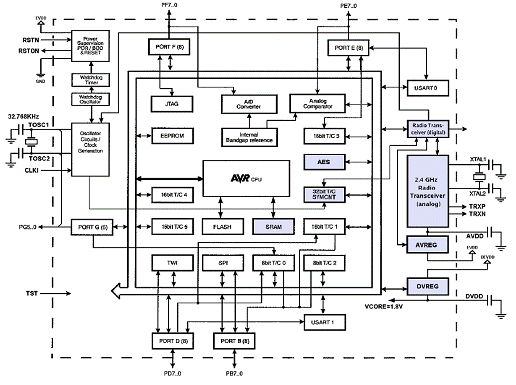
еӣҫ1.ATmega128RFA1ж–№жЎҶеӣҫ
The main function of the CPU core is to ensure correct program execution. The CPU must therefore be able to access memories, perform calculation, control peripherals, and handle interrupts.
In order to maximize performance and parallelism, the AVR uses a Harvard architecture вҖ“ with separate memories and buses for program and data. Instructions in the program memory are executed with a single level pipelining. While one instruction is being executed, the next instruction is pre-fetched from the program memory. This concept enables instructions to be executed in every clock cycle. The program memory is In-System Reprogrammable Flash memory.
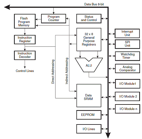
еӣҫ2.ATmega128RFA1зҡ„AVRжһ¶жһ„ж–№жЎҶеӣҫ
The ATmega128RFA1 features a low-power 2.4 GHz radio transceiver designed for industrial and consumer ZigBee/IEEE 802.15.4, 6LoWPAN, RF4CE and high data rate 2.4 GHz ISM band applications. The radio transceiver is a true peripheral block of the AVR microcontroller. All RF-critical components except the antenna, crystal and decoupling capacitors are integrated on-chip. Therefore, the ATmega128RFA1 is particularly suitable for applications like:
2.4 GHz IEEE 802.15.4 and ZigBee systems
6LoWPAN and RF4CE systems
Wireless sensor networks
Industrial control, sensing and automation (SP100, WirelessHART)
Residential and commercial automation
Health care
Consumer electronics
PC peripherals
Low-Power 2.4 GHz Transceiver Features
High performance RF-CMOS 2.4 GHz radio transceiver targeted for IEEE 802.15.4™, ZigBee™, IPv6 / 6LoWPAN, RF4CE, SP100, WirelessHART™ and ISM applications
Outstanding link budget (103.5 dB):
Receiver sensitivity -100 dBm
Programmable output power from -17 dBm up to +3.5 dBm
Ultra-low current consumption:
TRX_OFF = 0.4 mA
RX_ON = 12.5 mA
BUSY_TX = 14.5 mA (at max. transmit power of +3.5 dBm)
Optimized for low BoM cost and ease of production:
Few external components necessary (crystal, capacitors and antenna)
Excellent ESD robustness
Easy to use interface:
Registers and frame buffer access from software
Dedicated radio transceiver interrupts
Radio transceiver features:
128 byte FIFO (SRAM) for data buffering
Integrated RX/TX switch
Fully integrated, fast settling PLL to support frequency hopping
Battery monitor
Fast wake-up time < 0.25 ms
Special IEEE 802.15.4 2006 hardware support:
FCS computation and clear channel assessment (CCA)
RSSI measurement, energy detection and link quality indication
MAC hardware accelerator:
Automated acknowledgement, CSMA-CA and frame retransmission
Automatic address filtering
Automated FCS check
Extended Feature Set Hardware Support:
AES 128 bit hardware accelerator
RX/TX indication (external RF front-end control)
RX antenna diversity
Supported PSDU data rates: 250 kb/s, 500 kb/s, 1 Mb/s and 2 Mb/s
True random number generation for security applications
Compliant to IEEE 802.15.4-2006, IEEE 802.15.4-2003 and RF4CE
Compliant to EN 300 328/440, FCC-CFR-47 Part 15, ARIB STD-66, RSS-210
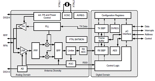
еӣҫ3.ATmega128RFA1收еҸ‘еҷЁж–№жЎҶеӣҫ
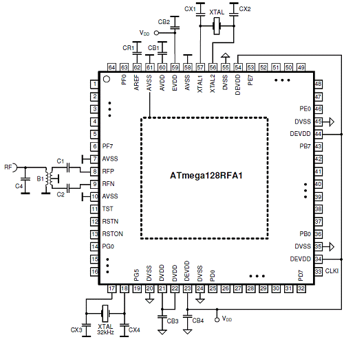
еӣҫ4.ATmega128RFA1еҹәжң¬еә”з”Ёз”өи·Ҝеӣҫ
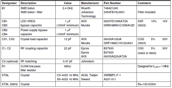
The 50 ohm single-ended RF input is transformed to the 100differential RF port impedance using Balun B1. The capacitors C1 and C2 provide AC coupling of the RF input to the RF port, capacitor C4 improves matching.
The power supply bypass capacitors (CB2, CB4) are connected to the external analog supply pin (EVDD, pin 59) and external digital supply pin (DEVDD, pin 23). Pins 34, 44 and 54 supply the digital port pins.
Capacitors CB1 and CB3 are bypass capacitors for the integrated analog and digital voltage regulators to ensure stable operation and to improve noise immunity.
Capacitors should be placed as close as possible to the pins and should have a low resistance and low-inductance connection to ground to achieve the best performance.
The crystal (XTAL), the two load capacitors (CX1, CX2), and the internal circuitry connected to pins XTAL1 and XTAL2 form the 16MHz crystal oscillator for the 2.4GHz transceiver. To achieve the best accuracy and stability of the reference frequency, large parasitic capacitances must be avoided. Crystal lines should be routed as short as possible and not in proximity of digital I/O signals. This is especially required for the High Data Rate Modes.
еҹәжң¬еә”з”Ёз”өи·Ҝжқҗж–ҷжё…еҚ•(BOM)
The ATmega128RFA1 supports additional features like:
Security Module (AES)
High Data Rate Mode up to 2MBits/s
Antenna Diversity using alternate pin function DIG1/2 at Port G and F
RX/TX Indicator using alternate pin function DIG3/4 at Port G and F
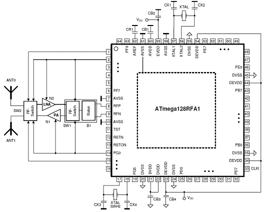
еӣҫ5.ATmega128RFA1жү©еұ•зү№жҖ§зҡ„еә”з”Ёз”өи·Ҝеӣҫ
The ATmega128RFA1-EK1 evaluation kit enables development, debugging and demonstration of IEEE 802.15.4 compliant wireless applications such as ZigBee� and 6LoWPAN. The kit contains two evaluation boards for ATmega128RFA1 covering the 2.4GHz ISM bands for use with STK600.

еӣҫ6. ATmega128RFA1-EK1иҜ„дј°жқҝеӨ–еҪўеӣҫ
иҜҰжғ…иҜ·и§Ғ:
http://www.atmel.com/dyn/resources/prod_documents/doc8266.pdf
The ATmega128RFA1 is a low-power CMOS 8 bit microcontroller based on the AVR
enhanced RISC architecture combined with a high data rate transceiver for the 2.4 GHz
ISM band. It is derived from the ATmega1281 microcontroller and the AT86RF231 radio
transceiver.
By executing powerful instructions in a single clock cycle, the device achieves throughputs approaching 1 MIPS per MHz allowing the system designer to optimize power consumption versus processing speed.
The radio transceiver provides high data rates from 250 kb/s up to 2 Mb/s, frame handling, outstanding receiver sensitivity and high transmit output power enabling a very robust wireless communication.
The AVR core combines a rich instruction set with 32 general purpose working registers. All 32 registers are directly connected to the Arithmetic Logic Unit (ALU). Two independent registers can be accessed with one single instruction executed in one clock cycle. The resulting architecture is very code efficient while achieving throughputs up to ten times faster than conventional CISC microcontrollers. The system includes internal voltage regulation and an advanced power management. Distinguished by the small leakage current it allows an extended operation time from battery.
The radio transceiver is a fully integrated ZigBee solution using a minimum number of external components. It combines excellent RF performance with low cost, small size and low current consumption. The radio transceiver includes a crystal stabilized fractional-N synthesizer, transmitter and receiver, and full Direct Sequence Spread Spectrum Signal (DSSS) processing with spreading and despreading. The device is fully compatible with IEEE802.15.4-2006/2003 and ZigBee standards.
ATmega128RFA1дё»иҰҒзү№жҖ§:
• High Performance, Low Power AVR® 8-Bit Microcontroller
• Advanced RISC Architecture
- 135 Powerful InstructionsвҖ“Most Single Clock Cycle Execution
- 32x8 General Purpose Working Registers
- Fully Static Operation
- Up to 16 MIPS Throughput at 16 MHz and 1.8V
- On-Chip 2-cycle Multiplier
• Non-volatile Program and Data Memories
- 128K Bytes of In-System Self-Programmable Flash
• Endurance: 2000 Write/Erase Cycles @ 85в„ғ
- 4K Bytes EEPROM
• Endurance: 2000 Write/Erase Cycles @ 85в„ғ
- 16K Bytes Internal SRAM
• JTAG (IEEE std. 1149.1 compliant) Interface
- Boundary-scan Capabilities According to the JTAG Standard
- Extensive On-chip Debug Support
- Programming of Flash EEPROM, Fuses and Lock Bits through the JTAG interface
• Peripheral Features
- Multiple Timer/Counter & PWM channels
- Real Time Counter with Separate Oscillator
- 10-bit, 330 ks/s A/D Converter; Analog Comparator; On-chip Temperature Sensor
- Master/Slave SPI Serial Interface
- Two Programmable Serial USART
- Byte Oriented 2-wire Serial Interface
• Advanced Interrupt Handler
• Watchdog Timer with Separate On-Chip Oscillator
• Power-on Reset and Low Current Brown-Out Detector
• Advanced Power Save Modes
• Fully integrated Low Power Transceiver for 2.4 GHz ISM Band
- Supported Data Rates: 250 kb/s and 500 kb/s,1 Mb/s, 2 Mb/s
- -100 dBm RX Sensitivity; TX Output Power up to 3.5 dBm
- Hardware Assisted MAC (Auto-Acknowledge, Auto-Retry)
- 32 Bit IEEE 802.15.4 Symbol Counter
- Baseband Signal Processing
- SFR-Detection, Spreading; De-Spreading; Framing ; CRC-16 Computation
- Antenna Diversity and TX/RX control
- TX/RX 128 Byte Frame Buffer
• Hardware Security (AES, True Random Generator)
• Integrated Crystal Oscillators (32.768 kHz & 16 MHz)
• I/O and Package
- 38 Programmable I/O Lines
- 64-pad QFN (RoHS/Fully Green)
• Temperature Range: -40в„ғ to 85в„ғ Industrial
• Supply voltage range 1.8V to 3.6V with integrated voltage regulators
• Ultra Low Power consumption (1.8 to 3.6V) for Rx/Tx & AVR: <18.6 mA
- CPU Active Mode (16MHz): 4.1 mA
- 2.4GHz Transceiver: RX_ON 12.5 mA/TX 14.5 mA (maximum TX output power)
- Deep Sleep Mode:<250nA @ 25в„ғ
• Speed Grade: 0вҖ“16 MHz @ 1.8вҖ“3.6V
ATmega128RFA1еә”з”Ё:
• ZigBee®/IEEE 802.15.4-2006/2003™вҖ“Full And Reduced Function Device (FFD/RFD)
• General Purpose 2.4GHz ISM Band Transceiver with Microcontroller
• RF4CE, SP100, WirelessHART™, ISM Applications and IPv6 / 6LoWPAN

еӣҫ1.ATmega128RFA1ж–№жЎҶеӣҫ
The main function of the CPU core is to ensure correct program execution. The CPU must therefore be able to access memories, perform calculation, control peripherals, and handle interrupts.
In order to maximize performance and parallelism, the AVR uses a Harvard architecture вҖ“ with separate memories and buses for program and data. Instructions in the program memory are executed with a single level pipelining. While one instruction is being executed, the next instruction is pre-fetched from the program memory. This concept enables instructions to be executed in every clock cycle. The program memory is In-System Reprogrammable Flash memory.

еӣҫ2.ATmega128RFA1зҡ„AVRжһ¶жһ„ж–№жЎҶеӣҫ
The ATmega128RFA1 features a low-power 2.4 GHz radio transceiver designed for industrial and consumer ZigBee/IEEE 802.15.4, 6LoWPAN, RF4CE and high data rate 2.4 GHz ISM band applications. The radio transceiver is a true peripheral block of the AVR microcontroller. All RF-critical components except the antenna, crystal and decoupling capacitors are integrated on-chip. Therefore, the ATmega128RFA1 is particularly suitable for applications like:
2.4 GHz IEEE 802.15.4 and ZigBee systems
6LoWPAN and RF4CE systems
Wireless sensor networks
Industrial control, sensing and automation (SP100, WirelessHART)
Residential and commercial automation
Health care
Consumer electronics
PC peripherals
Low-Power 2.4 GHz Transceiver Features
High performance RF-CMOS 2.4 GHz radio transceiver targeted for IEEE 802.15.4™, ZigBee™, IPv6 / 6LoWPAN, RF4CE, SP100, WirelessHART™ and ISM applications
Outstanding link budget (103.5 dB):
Receiver sensitivity -100 dBm
Programmable output power from -17 dBm up to +3.5 dBm
Ultra-low current consumption:
TRX_OFF = 0.4 mA
RX_ON = 12.5 mA
BUSY_TX = 14.5 mA (at max. transmit power of +3.5 dBm)
Optimized for low BoM cost and ease of production:
Few external components necessary (crystal, capacitors and antenna)
Excellent ESD robustness
Easy to use interface:
Registers and frame buffer access from software
Dedicated radio transceiver interrupts
Radio transceiver features:
128 byte FIFO (SRAM) for data buffering
Integrated RX/TX switch
Fully integrated, fast settling PLL to support frequency hopping
Battery monitor
Fast wake-up time < 0.25 ms
Special IEEE 802.15.4 2006 hardware support:
FCS computation and clear channel assessment (CCA)
RSSI measurement, energy detection and link quality indication
MAC hardware accelerator:
Automated acknowledgement, CSMA-CA and frame retransmission
Automatic address filtering
Automated FCS check
Extended Feature Set Hardware Support:
AES 128 bit hardware accelerator
RX/TX indication (external RF front-end control)
RX antenna diversity
Supported PSDU data rates: 250 kb/s, 500 kb/s, 1 Mb/s and 2 Mb/s
True random number generation for security applications
Compliant to IEEE 802.15.4-2006, IEEE 802.15.4-2003 and RF4CE
Compliant to EN 300 328/440, FCC-CFR-47 Part 15, ARIB STD-66, RSS-210

еӣҫ3.ATmega128RFA1收еҸ‘еҷЁж–№жЎҶеӣҫ

еӣҫ4.ATmega128RFA1еҹәжң¬еә”з”Ёз”өи·Ҝеӣҫ
The 50 ohm single-ended RF input is transformed to the 100differential RF port impedance using Balun B1. The capacitors C1 and C2 provide AC coupling of the RF input to the RF port, capacitor C4 improves matching.
The power supply bypass capacitors (CB2, CB4) are connected to the external analog supply pin (EVDD, pin 59) and external digital supply pin (DEVDD, pin 23). Pins 34, 44 and 54 supply the digital port pins.
Capacitors CB1 and CB3 are bypass capacitors for the integrated analog and digital voltage regulators to ensure stable operation and to improve noise immunity.
Capacitors should be placed as close as possible to the pins and should have a low resistance and low-inductance connection to ground to achieve the best performance.
The crystal (XTAL), the two load capacitors (CX1, CX2), and the internal circuitry connected to pins XTAL1 and XTAL2 form the 16MHz crystal oscillator for the 2.4GHz transceiver. To achieve the best accuracy and stability of the reference frequency, large parasitic capacitances must be avoided. Crystal lines should be routed as short as possible and not in proximity of digital I/O signals. This is especially required for the High Data Rate Modes.
еҹәжң¬еә”з”Ёз”өи·Ҝжқҗж–ҷжё…еҚ•(BOM)

The ATmega128RFA1 supports additional features like:
Security Module (AES)
High Data Rate Mode up to 2MBits/s
Antenna Diversity using alternate pin function DIG1/2 at Port G and F
RX/TX Indicator using alternate pin function DIG3/4 at Port G and F

еӣҫ5.ATmega128RFA1жү©еұ•зү№жҖ§зҡ„еә”з”Ёз”өи·Ҝеӣҫ
The ATmega128RFA1-EK1 evaluation kit enables development, debugging and demonstration of IEEE 802.15.4 compliant wireless applications such as ZigBee� and 6LoWPAN. The kit contains two evaluation boards for ATmega128RFA1 covering the 2.4GHz ISM bands for use with STK600.

еӣҫ6. ATmega128RFA1-EK1иҜ„дј°жқҝеӨ–еҪўеӣҫ
иҜҰжғ…иҜ·и§Ғ:
http://www.atmel.com/dyn/resources/prod_documents/doc8266.pdf
继з»ӯйҳ…иҜ»пјҡ
MicrochipеңЁзәҝе•Ҷеә—зҺ°е…Ёйқўдҫӣеә”жүҖжңүAtmelеҺҹжңүдә§е“Ғ
Atmelдёҡз•ҢжңҖдҪҺеҠҹиҖ—и“қзүҷжҷәиғҪи§ЈеҶіж–№жЎҲжү№йҮҸдёҠеёӮ
Atmel BitCloud ZigBee PROиҪҜ件ејҖеҸ‘е·Ҙе…·еҢ…иҺ·еҫ—вҖңй»„йҮ‘еҚ•е…ғвҖқиө„иҙЁ
AtmelдҪҺеҠҹиҖ—и“қзүҷжҷәиғҪж–№жЎҲеҠҹиҖ—жӣҙдҪҺ30%
Atmelе’ҢSIGFOXеңЁиҝңзЁӢзү©иҒ”зҪ‘иҝһжҺҘйўҶеҹҹејҖеұ•еҗҲдҪң

 зІӨе…¬зҪ‘е®үеӨҮ 44030902003195еҸ·