Jennic 公的JN5148是超低功耗高性能无线控制器,目标应用于 ZigBee PRO网络.器件采用增强的32位RISC处理器, 集成了2.4GHz IEEE802.15.4兼容的收发器,128KB ROM, 128KB RAM,以及各种丰富的模拟和数字接口. JN5148具有28位AES安全处理器,MAC加速器,500和667kbps数据速率,工作电压2.0V到3.6V,主要应用在ZigBee PRO网络,智能读表如AMR,家庭和建筑物自动化,工业系数,远程信息处理,遥控,游戏外设等.本文介绍了JN5148主要特性,方框图, 单端无线电架构图, 基带处理器框图, 安全处理器架构, SPI外设连接图, 定时器单元和UART方框图, 模拟外设方框图和PCB天线参考模块电路图以及元件列表.
The JN5148-001 is an ultra low power, high performance wireless microcontroller targeted at ZigBee PRO networking applications. The device features an enhanced 32-bit RISC processor offering high coding efficiency through variable width instructions, a multi-stage instruction pipeline and low power operation with programmable clock speeds. It also includes a 2.4GHz IEEE802.15.4 compliant transceiver, 128kB of ROM, 128kB of RAM, and a rich mix of analogue and digital peripherals. The large memory footprint allows the device to run both a network stack, e.g. ZigBee PRO, and an embedded application or in a co-processor mode. The operating current is below 18mA, allowing operation direct from a coin cell.
Enhanced peripherals include low power pulse counters running in sleep mode designed for pulse counting in AMR applications and a unique Time of Flight ranging engine, allowing accurate location services to be implemented on wireless sensor networks. It also includes a 4-wire I2S audio interface, to interface directly to mainstream audio CODECs, as well as conventional MCU peripherals.
JN5148主要特性:收发器
• 2.4GHz IEEE802.15.4 compliant
• Time of Flight ranging engine
• 128-bit AES security processor
• MAC accelerator with packet formatting, CRCs, address check, auto-acks, timers
• 500 & 667kbps data rate modes
• Integrated sleep oscillator for low power
• On chip power regulation for 2.0V to 3.6V battery operation
• Deep sleep current 100nA
• Sleep current with active sleep timer 1.25μA
• <$0.50 external component cost
• Rx current 17.5mA
• Tx current 15.0mA
• Receiver sensitivity -95dBm
• Transmit power 2.5dBm
MCU特性:
• Low power 32-bit RISC CPU, 4 to 32MHz clock speed
• Variable instruction width for high coding efficiency
• Multi-stage instruction pipeline
• 128kB ROM and 128kB RAM for bootloaded program code & data
• JTAG debug interface
• 4-input 12-bit ADC, 2 12-bit DACs, 2 comparators
• 3 application timer/counters,
• 2 UARTs
• SPI port with 5 selects
• 2-wire serial interface
• 4-wire digital audio interface
• Watchdog timer
• Low power pulse counters
• Up to 21 DIO
主要优势:
• Single chip integrates transceiver and microcontroller for wireless sensor networks
• Large memory footprint to run ZigBee PRO together with an application
• Very low current solution for long battery life
• Highly featured 32-bit RISC CPU for high performance and low power
• System BOM is low in component count and cost
• Extensive user peripherals
JN5148主要应用:
• Robust and secure low power wireless applications
• ZigBee PRO networks
• Smart metering (e.g. AMR)
• Home and commercial building automation
• Location Aware services – e.g. Asset Tracking
• Industrial systems
• Telemetry
• Remote Control
• Toys and gaming peripherals

图1.JN5148 方框图
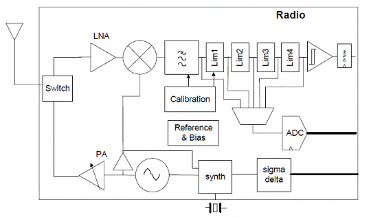
图2.JN5148单端无线电架构图
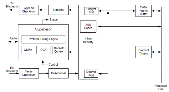
图3.JN5148基带处理器框图

图4.JN5148安全处理器架构
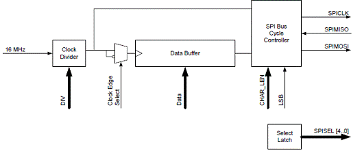
图5.JN5148 SPI方框图
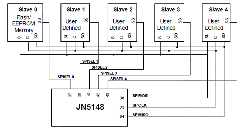
图6.JN5148典型SPI外设连接图

图7.JN5148定时器单元方框图
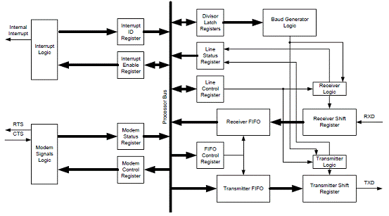
图8.JN5148 UART方框图
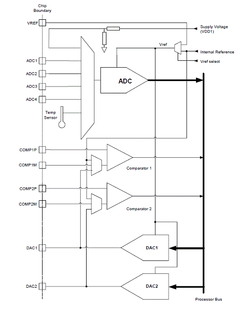
图9.JN5148模拟外设方框图
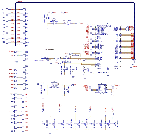
图10.JN5148 PCB天线参考模块电路图
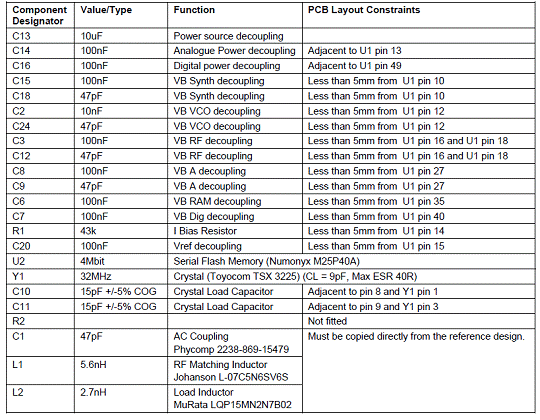
JN5148 PCB天线参考模块电路图元件列表
详情请见:
http://www.jennic.com/download_file.php?brief=JN-DS-JN5148-1v2.pdf
The JN5148-001 is an ultra low power, high performance wireless microcontroller targeted at ZigBee PRO networking applications. The device features an enhanced 32-bit RISC processor offering high coding efficiency through variable width instructions, a multi-stage instruction pipeline and low power operation with programmable clock speeds. It also includes a 2.4GHz IEEE802.15.4 compliant transceiver, 128kB of ROM, 128kB of RAM, and a rich mix of analogue and digital peripherals. The large memory footprint allows the device to run both a network stack, e.g. ZigBee PRO, and an embedded application or in a co-processor mode. The operating current is below 18mA, allowing operation direct from a coin cell.
Enhanced peripherals include low power pulse counters running in sleep mode designed for pulse counting in AMR applications and a unique Time of Flight ranging engine, allowing accurate location services to be implemented on wireless sensor networks. It also includes a 4-wire I2S audio interface, to interface directly to mainstream audio CODECs, as well as conventional MCU peripherals.
JN5148主要特性:收发器
• 2.4GHz IEEE802.15.4 compliant
• Time of Flight ranging engine
• 128-bit AES security processor
• MAC accelerator with packet formatting, CRCs, address check, auto-acks, timers
• 500 & 667kbps data rate modes
• Integrated sleep oscillator for low power
• On chip power regulation for 2.0V to 3.6V battery operation
• Deep sleep current 100nA
• Sleep current with active sleep timer 1.25μA
• <$0.50 external component cost
• Rx current 17.5mA
• Tx current 15.0mA
• Receiver sensitivity -95dBm
• Transmit power 2.5dBm
MCU特性:
• Low power 32-bit RISC CPU, 4 to 32MHz clock speed
• Variable instruction width for high coding efficiency
• Multi-stage instruction pipeline
• 128kB ROM and 128kB RAM for bootloaded program code & data
• JTAG debug interface
• 4-input 12-bit ADC, 2 12-bit DACs, 2 comparators
• 3 application timer/counters,
• 2 UARTs
• SPI port with 5 selects
• 2-wire serial interface
• 4-wire digital audio interface
• Watchdog timer
• Low power pulse counters
• Up to 21 DIO
主要优势:
• Single chip integrates transceiver and microcontroller for wireless sensor networks
• Large memory footprint to run ZigBee PRO together with an application
• Very low current solution for long battery life
• Highly featured 32-bit RISC CPU for high performance and low power
• System BOM is low in component count and cost
• Extensive user peripherals
JN5148主要应用:
• Robust and secure low power wireless applications
• ZigBee PRO networks
• Smart metering (e.g. AMR)
• Home and commercial building automation
• Location Aware services – e.g. Asset Tracking
• Industrial systems
• Telemetry
• Remote Control
• Toys and gaming peripherals

图1.JN5148 方框图

图2.JN5148单端无线电架构图

图3.JN5148基带处理器框图

图4.JN5148安全处理器架构

图5.JN5148 SPI方框图

图6.JN5148典型SPI外设连接图

图7.JN5148定时器单元方框图

图8.JN5148 UART方框图

图9.JN5148模拟外设方框图

图10.JN5148 PCB天线参考模块电路图
JN5148 PCB天线参考模块电路图元件列表

详情请见:
http://www.jennic.com/download_file.php?brief=JN-DS-JN5148-1v2.pdf

 粤公网安备 44030902003195号