Atmel е…¬еҸёзҡ„AT86RF212жҳҜдҪҺеҠҹиҖ—дҪҺз”өеҺӢ700/800/900 MHz 收еҸ‘еҷЁ,зү№еҲ«и®ҫи®Ўз”ЁдәҺIEEE Standard 802.15.4, ZigBee, 6LoWPANд»ҘеҸҠй«ҳж•°жҚ®йҖҹзҺҮISMеә”з”Ё. AT86RF212еҚ•зүҮRF收еҸ‘еҷЁжҸҗдҫӣдәҶеӨ©зәҝе’Ңеҫ®жҺ§еҲ¶еҷЁй—ҙе®Ңж•ҙжҺҘеҸЈ,еҢ…жӢ¬жңүжЁЎжӢҹж— зәҝз”өйғЁеҲҶ,еҢ…жӢ¬ж—¶й—ҙе’Ңйў‘зҺҮеҗҢжӯҘзҡ„ж•°еӯ—и°ғеҲ¶е’Ңи§Ји°ғ, д»ҘеҸҠж•°жҚ®зј“еҶІеҠҹиғҪ.жҺҘ收зҒөж•ҸеәҰй«ҳиҫҫ-110dBm,еҸҜзј–зЁӢTXиҫ“еҮәеҠҹзҺҮй«ҳиҫҫ+10dBm,е·ҘдҪңз”өеҺӢд»Һ1.8VеҲ°3.6V,еҶ…йғЁжңүз”өеҺӢзЁіеҺӢеҷЁе’Ңз”өжұ зӣ‘и§ҶеҷЁ,е·ҘдҪңжё©еәҰ-40еәҰCеҲ°85еәҰC.жң¬ж–Үд»Ӣз»ҚдәҶAT86RF212зҡ„дё»иҰҒзү№жҖ§е’Ңж–№жЎҶеӣҫ,д»ҘеҸҠеҹәжң¬еә”з”Ёз”өи·Ҝеӣҫе’ҢжүҖз”Ёзҡ„жқҗж–ҷжё…еҚ•.жӯӨеӨ–иҝҳд»Ӣз»ҚдәҶжү©еұ•зү№жҖ§еә”з”Ёз”өи·Ҝеӣҫ.
The AT86RF212 is a low-power, low-voltage 700/800/900 MHz transceiver specially
designed for the IEEE Standard 802.15.4, ZigBee, 6LoWPAN, and high data rate ISM
applications. For the sub-1 GHz bands, it supports low data rates (20 and 40 kbit/s) of
the IEEE Standard 802.15.4-2003 [2] and provides optional data rates (100 and 250
kbit/s) using O-QPSK, according to the IEEE Standard 802.15.4-2006 [1] and the
respective IEEE P802.15.4c Draft Amendment [3]. Furthermore, proprietary High Data
Rate Modes up to 1000 kbit/s can be employed.
The AT86RF212 is a true SPI-to-antenna solution. RF-critical components except the
antenna, crystal, and de-coupling capacitors are integrated on-chip. MAC and AES
hardware accelerators improve overall system power efficiency and timing.
The AT86RF212 single-chip RF transceiver provides a complete radio interface
between the antenna and the microcontroller. It comprises the analog radio part, digital
modulation and demodulation including time and frequency synchronization, as well as
data buffering. The number of external components is minimized so that only the
antenna, a filter (at high output power levels), the crystal, and four bypass capacitors
are required. The bidirectional differential antenna pins are used in common for RX and
TX, i.e. no external antenna switch is needed. Control of an external power amplifier is
supported by two digital control signals (differential operation).
The receiver path is based on a low-IF architecture. After channel filtering and downconversion the low-IF signal is sampled and applied to the digital signal processing part. Communication between transmitter and receiver is based on direct sequence spread spectrum with different modulation schemes and spreading codes. The AT86RF212 supports the IEEE 802.15.4-2006 standard mandatory BPSK modulation and optional O-QPSK modulation in the 868.3 MHz and 915 MHz bands. In addition it supports the O-QPSK modulation defined in IEEE P802.15.4c for the Chinese 780 MHz band.
For applications not necessarily targeting IEEE compliant networks the radio transceiver supports proprietary High Data Rate Modes based on O-QPSK. A single 128 byte TRX buffer stores receive or transmit data. The AT86RF212 features hardware supported 128 bit security operation. The standalone AES encryption/decryption engine can be accessed in parallel to all PHY operational modes. Configuration of the AT86RF212, reading, and writing of data memory as well as the AES hardware engine are controlled by the SPI interface and additional control signals.
On-chip low-dropout voltage regulators provide the analog and digital 1.8 V power supply. Control registers retain their settings in SLEEP mode when the regulators are turned off. The RX and TX signal processing paths are highly integrated and optimized for low power consumption.
AT86RF212дё»иҰҒзү№жҖ§:
Fully Integrated 700/800/900 MHz-Band Transceiver
Chinese WPAN Band from 779 to 787 MHz
European SRD Band from 863 to 870 MHz
North American ISM Band from 902 to 928 MHz
Direct Sequence Spread Spectrum with Different Modulation Schemes and Data Rates
BPSK with 20 and 40 kbit/s, compliant to IEEE 802.15.4-2006
O-QPSK with 100 and 250 kbit/s, compliant to IEEE 802.15.4-2006
O-QPSK with 250 kbit/s, compliant to IEEE P802.15.4c
O-QPSK with 200, 400, 500, and 1000 kbit/s PSDU Data Rate
Flexible Combination of Frequency Bands and Data Rates
Industry Leading Link Budget
Receiver Sensitivity up to -110 dBm
Programmable TX Output Power up to +10 dBm
Low Power Supply Voltage from 1.8 V to 3.6 V
Internal Voltage Regulators and Battery Monitor
Low Current Consumption
SLEEP = 0.2 ОјA
TRX_OFF = 0.4 mA
RX_ON = 9.0 mA
BUSY_TX = 18 mA at PTX = 5 dBm
Digital Interface
Registers, Frame Buffer, and AES Accessible through SPI
Clock Output with Configurable Rate
Radio Transceiver Features
Adjustable Receiver Sensitivity
Integrated TX/RX Switch, LNA, and PLL Loop Filter
Fast Settling PLL Supporting Frequency Hopping
Automatic VCO and Filter Calibration
Integrated 16 MHz Crystal Oscillator
128 byte FIFO for Transmit/Receive
IEEE 802.15.4-2006 Hardware Support
FCS Computation and Check
Clear Channel Assessment
Received Signal Strength Indicator, Energy Detection, and Link Quality Indication
MAC Hardware Accelerator
Automatic Acknowledgement and Retransmission
CSMA-CA and LBT
Automatic Frame Filtering
AES 128 bit Hardware Accelerator (ECB and CBC modes)
Extended Feature Set Hardware Support
True Random Number Generation for Security Applications
TX/RX Indication (External RF Front End Control)
Optimized for Low BoM Cost and Ease of Production
Low External Component Count: Antenna, Reference Crystal, and Bypass Capacitors
Excellent ESD Robustness
Industrial Temperature Range from -40В°C to +85В°C
32-pin Low-profile Lead-free Plastic QFN Package, 5.0 x 5.0 x 0.9 mm3
Compliant to IEEE 802.15.4-2003, IEEE 802.15.4-2006, IEEE P802.15.4c, ETSI EN 300 220-1, and FCC 47 CFR Section 15.247
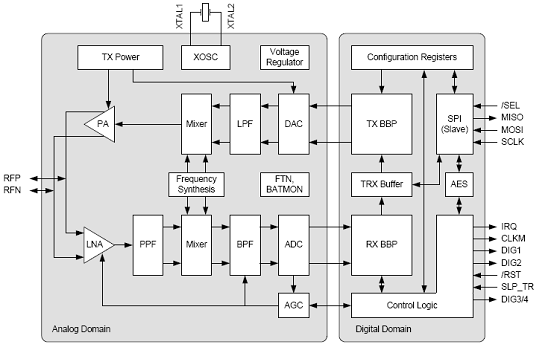
еӣҫ1.AT86RF212 ж–№жЎҶеӣҫ
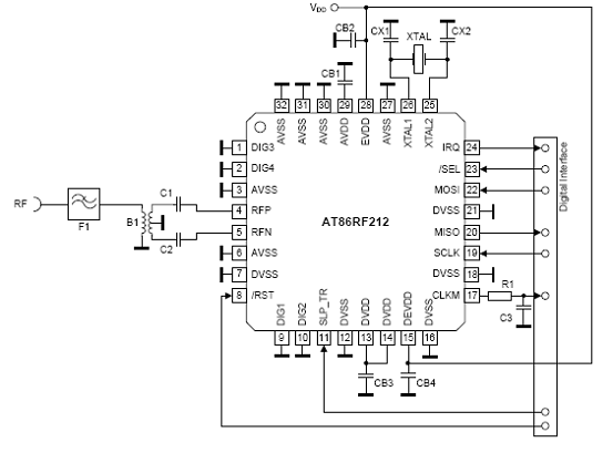
еӣҫ2.AT86RF212еҹәжң¬еә”з”Ёз”өи·Ҝеӣҫ
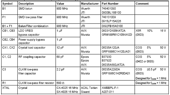
еҹәжң¬еә”з”Ёз”өи·Ҝеӣҫдёӯзҡ„жқҗж–ҷжё…еҚ•(BOM):
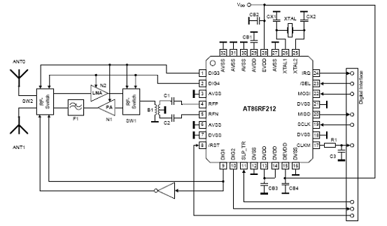
еӣҫ3. AT86RF212жү©еұ•зү№жҖ§еә”з”Ёз”өи·Ҝеӣҫ
иҜҰжғ…иҜ·и§Ғ:
http://www.atmel.com/dyn/resources/prod_documents/doc8168.pdf
The AT86RF212 is a low-power, low-voltage 700/800/900 MHz transceiver specially
designed for the IEEE Standard 802.15.4, ZigBee, 6LoWPAN, and high data rate ISM
applications. For the sub-1 GHz bands, it supports low data rates (20 and 40 kbit/s) of
the IEEE Standard 802.15.4-2003 [2] and provides optional data rates (100 and 250
kbit/s) using O-QPSK, according to the IEEE Standard 802.15.4-2006 [1] and the
respective IEEE P802.15.4c Draft Amendment [3]. Furthermore, proprietary High Data
Rate Modes up to 1000 kbit/s can be employed.
The AT86RF212 is a true SPI-to-antenna solution. RF-critical components except the
antenna, crystal, and de-coupling capacitors are integrated on-chip. MAC and AES
hardware accelerators improve overall system power efficiency and timing.
The AT86RF212 single-chip RF transceiver provides a complete radio interface
between the antenna and the microcontroller. It comprises the analog radio part, digital
modulation and demodulation including time and frequency synchronization, as well as
data buffering. The number of external components is minimized so that only the
antenna, a filter (at high output power levels), the crystal, and four bypass capacitors
are required. The bidirectional differential antenna pins are used in common for RX and
TX, i.e. no external antenna switch is needed. Control of an external power amplifier is
supported by two digital control signals (differential operation).
The receiver path is based on a low-IF architecture. After channel filtering and downconversion the low-IF signal is sampled and applied to the digital signal processing part. Communication between transmitter and receiver is based on direct sequence spread spectrum with different modulation schemes and spreading codes. The AT86RF212 supports the IEEE 802.15.4-2006 standard mandatory BPSK modulation and optional O-QPSK modulation in the 868.3 MHz and 915 MHz bands. In addition it supports the O-QPSK modulation defined in IEEE P802.15.4c for the Chinese 780 MHz band.
For applications not necessarily targeting IEEE compliant networks the radio transceiver supports proprietary High Data Rate Modes based on O-QPSK. A single 128 byte TRX buffer stores receive or transmit data. The AT86RF212 features hardware supported 128 bit security operation. The standalone AES encryption/decryption engine can be accessed in parallel to all PHY operational modes. Configuration of the AT86RF212, reading, and writing of data memory as well as the AES hardware engine are controlled by the SPI interface and additional control signals.
On-chip low-dropout voltage regulators provide the analog and digital 1.8 V power supply. Control registers retain their settings in SLEEP mode when the regulators are turned off. The RX and TX signal processing paths are highly integrated and optimized for low power consumption.
AT86RF212дё»иҰҒзү№жҖ§:
Fully Integrated 700/800/900 MHz-Band Transceiver
Chinese WPAN Band from 779 to 787 MHz
European SRD Band from 863 to 870 MHz
North American ISM Band from 902 to 928 MHz
Direct Sequence Spread Spectrum with Different Modulation Schemes and Data Rates
BPSK with 20 and 40 kbit/s, compliant to IEEE 802.15.4-2006
O-QPSK with 100 and 250 kbit/s, compliant to IEEE 802.15.4-2006
O-QPSK with 250 kbit/s, compliant to IEEE P802.15.4c
O-QPSK with 200, 400, 500, and 1000 kbit/s PSDU Data Rate
Flexible Combination of Frequency Bands and Data Rates
Industry Leading Link Budget
Receiver Sensitivity up to -110 dBm
Programmable TX Output Power up to +10 dBm
Low Power Supply Voltage from 1.8 V to 3.6 V
Internal Voltage Regulators and Battery Monitor
Low Current Consumption
SLEEP = 0.2 ОјA
TRX_OFF = 0.4 mA
RX_ON = 9.0 mA
BUSY_TX = 18 mA at PTX = 5 dBm
Digital Interface
Registers, Frame Buffer, and AES Accessible through SPI
Clock Output with Configurable Rate
Radio Transceiver Features
Adjustable Receiver Sensitivity
Integrated TX/RX Switch, LNA, and PLL Loop Filter
Fast Settling PLL Supporting Frequency Hopping
Automatic VCO and Filter Calibration
Integrated 16 MHz Crystal Oscillator
128 byte FIFO for Transmit/Receive
IEEE 802.15.4-2006 Hardware Support
FCS Computation and Check
Clear Channel Assessment
Received Signal Strength Indicator, Energy Detection, and Link Quality Indication
MAC Hardware Accelerator
Automatic Acknowledgement and Retransmission
CSMA-CA and LBT
Automatic Frame Filtering
AES 128 bit Hardware Accelerator (ECB and CBC modes)
Extended Feature Set Hardware Support
True Random Number Generation for Security Applications
TX/RX Indication (External RF Front End Control)
Optimized for Low BoM Cost and Ease of Production
Low External Component Count: Antenna, Reference Crystal, and Bypass Capacitors
Excellent ESD Robustness
Industrial Temperature Range from -40В°C to +85В°C
32-pin Low-profile Lead-free Plastic QFN Package, 5.0 x 5.0 x 0.9 mm3
Compliant to IEEE 802.15.4-2003, IEEE 802.15.4-2006, IEEE P802.15.4c, ETSI EN 300 220-1, and FCC 47 CFR Section 15.247

еӣҫ1.AT86RF212 ж–№жЎҶеӣҫ

еӣҫ2.AT86RF212еҹәжң¬еә”з”Ёз”өи·Ҝеӣҫ
еҹәжң¬еә”з”Ёз”өи·Ҝеӣҫдёӯзҡ„жқҗж–ҷжё…еҚ•(BOM):


еӣҫ3. AT86RF212жү©еұ•зү№жҖ§еә”з”Ёз”өи·Ҝеӣҫ
иҜҰжғ…иҜ·и§Ғ:
http://www.atmel.com/dyn/resources/prod_documents/doc8168.pdf
继з»ӯйҳ…иҜ»пјҡ
MicrochipеңЁзәҝе•Ҷеә—зҺ°е…Ёйқўдҫӣеә”жүҖжңүAtmelеҺҹжңүдә§е“Ғ
Atmelдёҡз•ҢжңҖдҪҺеҠҹиҖ—и“қзүҷжҷәиғҪи§ЈеҶіж–№жЎҲжү№йҮҸдёҠеёӮ
Atmel BitCloud ZigBee PROиҪҜ件ејҖеҸ‘е·Ҙе…·еҢ…иҺ·еҫ—вҖңй»„йҮ‘еҚ•е…ғвҖқиө„иҙЁ
AtmelдҪҺеҠҹиҖ—и“қзүҷжҷәиғҪж–№жЎҲеҠҹиҖ—жӣҙдҪҺ30%
Atmelе’ҢSIGFOXеңЁиҝңзЁӢзү©иҒ”зҪ‘иҝһжҺҘйўҶеҹҹејҖеұ•еҗҲдҪң

 зІӨе…¬зҪ‘е®үеӨҮ 44030902003195еҸ·