| 资料语言: | 英文 |
| 资料类别: | PDF文档 |
| 浏览次数: | 0 |
| 评论等级: | |
| 更新时间: | 2013-04-19 14:25:00 |
| 资料查询: |

WS8: Advanced Modeling Techniques for Carbon-Based RF and THz structures
Type: Half Day
Day/Date/Time: Thursday, 18 April 2013, 0830-1230
Location: Room 311B
Organizer:
Prof. Wen-Yan Yin, Zhejiang University, Shanghai Jiao Tong University
Abstract:
This workshop will be focused on some advanced modeling techniques for carbon-based RF and THz structures. It consists of five parts as given as follows:
(1) Carbon-Based Nanoelectronics: Device Physics, Modeling, and Simulation;
(2) Electronic Design Automation for Nano- Integrated Circuits;
(3) Development of Lumped-element Circuit Models for Carbon-based Passives and Actives for RF/THz Applications.
Title of each Presentation and the Author(s)/Affiliations:
Title 1: Carbon-Based Nanoelectronics: Device Physics, Modeling, and Simulation
Speaker: Prof. Jin Guo
University of Florida, USA
Abstract:
In recent years, significant progress has been achieved in graphene and carbon nanotube (CNT) electronics. In a graphene or carbon nanotube, low bias transport can be nearly ballistic. Deposition of high-k gate insulators does not degrade the carrier mobility because of an absence of dangling bonds. The conduction and valence bands are symmetric, which is advantageous for complementary applications. The Excellent transport property promises high-speed transistor applications. Carbon-based nanostructures are receiving much attention for possible device applications.
We have developed a self-consistent atomistic simulator for graphene and CNT field-effect transistors (FETs) based on the non-equilibrium Green’s function (NEGF) formalism, and applied it to understand experiments and to suggest design optimization. We show that a recently reported high-performance CNTFET delivers a near ballistic DC on-current even under high source-drain bias conditions. A method to assess how the CNTFET compares to the state-of-the-art Si MOSFET is developed. The radio frequency (RF) characteristics of CNTFETs are simulated for understanding potential high-speed transistor applications. On graphene electronics, we assess the RF performance limits of aggressively scaled graphene FETs in the presence of Klein tunneling, inelastic phonon scattering, and self-heating effects.
Title 2: Electronic Design Automation for Nano- Integrated Circuits
Speaker: Prof. ERPING LI
RF and Nanoelectronic Research Centre, Zhejiang University, China
Abstract:
Compact integrated nanophotonic devices promise both high speed and small dimensions for information processing. In recent years, it has been demonstrated theoretically and experimentally that propagating electromagnetic waves can be coupled into sub-wavelength photonic devices through surface plasmon polaritons, the technology of which is commonly referred to as nanoplasmonics. The efficient design of sub-wavelength nanoplasmonic components typically requires full-wave electromagnetic simulations for accurate characterization of the device at nano-scale, which may become quite costly in time and resource consuming. Recently, the equivalent transmission-line models and circuits have been vastly proposed to characterize several nanoplasmonic components. However, all these works focus on single component of nanoplasmonic circuit. For these reasons, System-Level Electronic Design Automation (EDA) tool integrating circuit representations of different components and being capable of modeling comprehensive nanoplasmonic circuits and systems would be highly desirable.
The purpose of this work is to propose a system-level circuit simulation framework for effectively modeling, design and optimizing nanoplasmonic components and circuits. The EDA environment, developed under Modelica language, provides an equivalent circuit model library for several nanoplasmonic Metal-Insulator-Metal based components. The accuracy of the equivalent models for the nanoplasmonic circuit library is verified by using full-wave simulations and analytical equations. These models are then used to design an ultra-compact Mach-Zehnder nanoplasmonic modulator. It is shown that the low voltage required to achieve an 180o-phase shift in the modulator can be predicted by the simulator with a high accuracy.
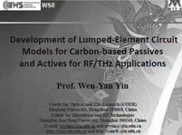
Title 3: Development of Lumped-element Circuit Models for Carbon-based Passives and Actives for RF/THz Applications
Speaker: Prof. Wen-Yan Yin
Center for Optical and Electromagnetic Research, Zhejiang University, Hangzhou, 310058, CHINA
Center for Microwave and RF Technologies, Shanghai Jiao Tong University, Shanghai, 200240, CHINA
Abstract:
More recently, significant progress has been achieved in the development of carbon-based (carbon nanotube (CNT) and graphene) interconnects and field effect transistors for future RF/THz integration and application.
In order to thoroughly understand signal transmission characteristics of single-, double-, multi-walled carbon nanotube (SWCNT & DWCNT& MWCNT) and few-layer graphene transmission lines as well as input-output responses of both CENTFET and GFET, we have to build up their lumped-element circuit models, where quantum effects should be treated in an appropriate way.
In this talk, circuit-oriented modeling technique will be employed for handling SWCNT, DWCNT, MWCNT, few-layer graphene nanoribbon transmission lines and active devices, where physics-based methodologies will be addressed for fast extracting all lumped elements (resistance, inductance, capacitance and conductance) . Further, both frequency- and temperature-dependent characteristics of these carbon-based structures can be understood and optimized for RF/ THz integrations.
温馨提示:本站不提供资料文件下载,仅提供文件名称查询,如有疑问请联系我们。


 粤公网安备 44030902003195号